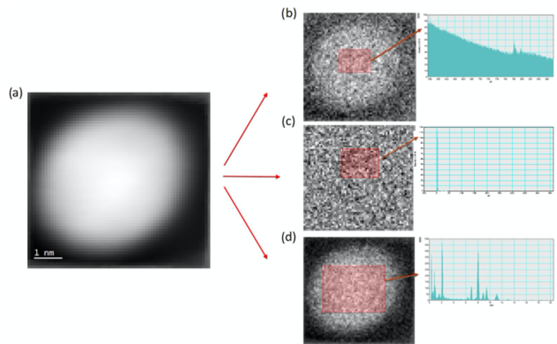
The overarching aim of this project is to quantitatively characterise bimetallic nanoparticles using the scanning transmission electron microscope (STEM). Using STEM, it is possible to collect ADF signals, EDS and EELS signals simultaneously from a nanoparticle. ADF signals can be used to obtain atomic positions as well as determine the size and shape of the nanoparticle, whereas EDS and EELS signals can be used to obtain information regarding composition.
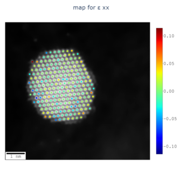
One of the objectives of this project is to measure the strain distribution on atomic resolution ADF images of bimetallic nanoparticles. With the assistance of computer programming, the strain distribution of those nanoparticles can be calculated and also used as inputs for DFT simulation.
Another objective is to analyze the compositional distribution of bimetallic nanoparticles. The spectroscopic signals from pure element standards, such as needles or nanoparticles, are required to calibrate partial cross-sections of single atoms. The aim is then to use these cross-sections to atom count bimetallic nanoparticles from EDS and EELS mapping.

Figure 2. The strain measurement on the atomic resolution ADF image of the PtCo nanoparticle

Figure 3. The simultaneous acquisition of ADF, EELS and EDS signals on the PtCo nanoparticle. (a) ADF image. (b) EELS core loss image. (c) EELS low loss image. (d) EDS image
The measured strain and compositional distribution of the nanoparticles can finally be related to the catalytic activity through theoretical DFT calculation.