The electronic structure of a material determines many of its essential properties, making a thorough understanding of this structure crucial for good materials science. Developments in theoretical, computational, and experimental techniques make probing the electronic structure of materials ever more practical and precise. On the theoretical/computational side, the methods of Hartree-Fock theory and density functional theory (DFT) have been very successful in making first-principles calculations of the electronic structure of many materials tractable. Experimentally, transmission electron microscopy (TEM), scanning transmission electron microscopy (STEM), and electron energy loss spectroscopy (EELS) offer quantitative methods of studying the electronic structure of materials. Furthering the integration of theoretical and computational electronic structure methods with STEM and EELS techniques is the overarching theme of my DPhil project.

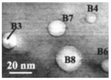
Figure 1: Experimental STEM image of helium bubbles in a silicon matrix.
Figure 2: Visualisation of projected potentials for hexagonal boron nitride. a) shows the projected potential of the IAM, while b) is the result of a full DFT calculation using CASTEP. In c) we see the difference between the two, resulting primarily from transfer of charge between boron and nitrogen atoms.